Two-dimensional atomic crystal is a new type of material, and research results are increasing
Two-dimensional atomic crystal is a new type of thin film material. The thickness of this crystal material is only one atom, like a huge two-dimensional molecule. Two-dimensional atomic crystals are obtained by peeling off single-layer crystals with a layered structure, and the peeling process is difficult. Two-dimensional atomic crystals have stable properties and can be used to manufacture field-effect transistors, gas sensors, translational motors, electromechanical equipment and other products.
Materials science is closely related to social development and has a great impact on the national economy, manufacturing development, and residents’ lives. With the continuous advancement of science and technology, the performance requirements for materials in the downstream market continue to increase. In order to meet the needs of the downstream market, materials with excellent performance and special properties New functional materials are constantly being developed and released. Two-dimensional atomic crystals are one type of new materials, and their research has attracted attention.
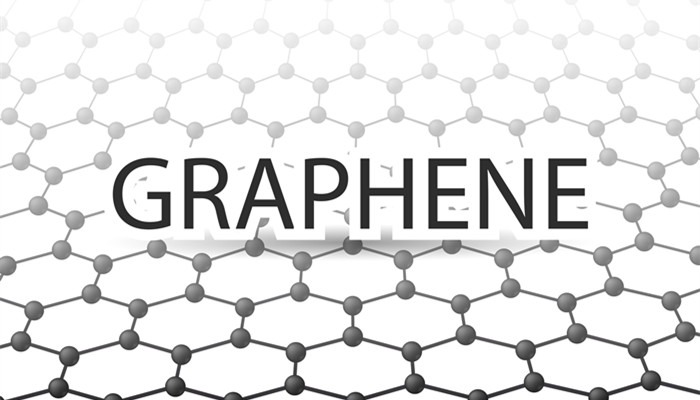
According to the “2021-2025 Two-dimensional Atomic Crystal Industry In-depth Market Research and Investment Strategy Suggestions Report” released by the Industrial Research Center, Two-dimensional atomic crystals were first developed by British and Russian scientists. They can be obtained by exfoliating graphite, graphene, boron nitride, hexagonal boron nitride, and some disulfides, oxides, etc. Among them, graphene and hexagonal nitride Boron has attracted a lot of attention. Graphene has excellent mechanical, optical, and electrical properties and is considered to be the new material most likely to change the world. Therefore, the research and development of its two-dimensional atomic crystals is very popular. The crystal structure and parameters of hexagonal boron nitride are similar to graphene. Hexagonal boron nitride can be used as a substrate, a graphene layer can be spread on it, and then used to manufacture electronic devices. Therefore, research and development is gradually increasing.
Since 2008, the development of the global new materials industry has accelerated. New materials have become an important basis for industrially developed countries to seize the commanding heights of a new round of international scientific and technological economic competition. my country is transforming from a manufacturing country to a manufacturing power. The government and capital are paying attention to new materials. The degree is high, relevant encouragement and support policies are continuously introduced, and capital investment is continuously increased, which jointly promote the continuous improvement of the output value of my country’s new materials industry. Preliminary estimates indicate that the output value of my country’s new materials industry will reach 6.8 trillion yuan in 2021, continuing to maintain rapid growth. Against this background, the two-dimensional atomic crystal industry has broad prospects for development.
Industry analysts said that the technical barriers to two-dimensional atomic crystals are high, and it is still in the technical research stage in my country, and relevant research results are constantly coming out. . In 2015, a team from the Institute of Semiconductors, Chinese Academy of Sciences, made a series of progress in the preparation of h-BN (hexagonal boron nitride) two-dimensional atomic crystals and graphene/h-BN heterojunctions. In 2017, a team from the Institute of Physics of the Chinese Academy of Sciences achieved a series of internationally cutting-edge research results in the preparation, physical properties and application basis of graphene and graphene-like two-dimensional atomic crystal materials. In 2020, the Institute of Physics of the Chinese Academy of Sciences/Beijing National Research Center for Condensed Matter Physics team made progress in the study of the Kondo effect of the two-dimensional atomic crystal VTe2.
In the “Nano Frontier” key project of my country’s “14th Five-Year Plan” national key research and development plan, terahertz and mid-far infrared band polariton two-dimensional atomic crystals and their sensing and storage micro-nano devices are included, which will further promote my country’s second Advances in dimensional atomic crystal research technology. In the future, while technological research continues to deepen, our country also needs to focus on the industrial transformation of two-dimensional atomic crystal research results.
 微信扫一扫打赏